The original DRAM took approximately six system-bus clock cycles for each memory access. During memory access, first the RAS and CAS and then 64 bits of data were transferred through the memory bus. The next sequential address access required a repeat of the RAS-CAS-Data sequence. As a result, most of the overhead occurred while transferring row and column addresses, rather than the data.
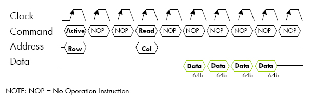
FPM and EDO improved performance by automatically retrieving data from sequential memory locations on the assumption that they would also be requested. Using this process called burst mode access, four consecutive 64-bit sections of memory are accessed, one after the other, based on the address of the first section. So instead of taking six clock cycles to access each of the last three 64-bit sections, it may take from one to three clock cycles each (see Figure 4).
Burst mode access timing is normally stated in the format �x-y-y-y� where �x� represents the number of clock cycles to read/write the first 64 bits and �y� represents the number of clock cycles required for the second, third, and fourth reads/writes. For example, prior to burst mode access, DRAM took up to 24 clock cycles (6-6-6-6) to access four 64-bit memory sections. With burst mode access, three additional data sections are accessed with every clock cycle after the first access (6-1-1-1) before the memory controller has to send another CAS.
Information porvided by Hewlett-Packard Development Company, L.P.
����˹��� RAM, SSD, HDD & Upgrade Parts ����Ѻ Server �ѹ�Ѻ 1 �ͧ������� !!
RAM and SSD -> Server, Workstation, Apple Mac, Notebook, Desktop PC : Server Options -> Processor, Memory, SAS HDD, Storage Controller, Power Supply, Spare Part
MemoryToday Co., Ltd. 7 IT-Mall Fortune Town Bldg., 3rd Floor, Room 3R22, Ratchadapisek Rd., Dindaeng, Bangkok 10400 Tel: 02-641-0055 Fax: 02-641-0066 Web site engine's code is Copyright by PHP-Nuke. All Rights Reserved. PHP-Nuke is Free Software released under the GNU/GPL license.